CNT active matrix makes flexible imager
作者:中國科學院成都有機化學有限公司 來源:http://www.sikpqwc.cn 日期:2013-11-27 09:02:06
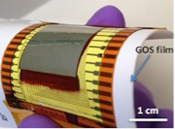
Researchers at the University of California, Berkeley, and the Lawrence Berkeley National Laboratory have succeeded in fabricating mechanically flexible imagers using nanotube-based active-matrix backplanes. The devices, which can image in both the visible and X-ray range, could be used to make large-area flexible sensor networks for a variety of imaging applications, such as interactive surfaces and displays that can be pasted onto a host of surfaces and objects. The devices that work in the X-ray part of the spectrum might find use in portable medical imaging too.
 川公網安備 51010702000618號
主站蜘蛛池模板:
国产精品久久久久久久久久久久
|
厕拍精品
|
国产精品高清视亚洲一区二区
|
fc2成年手机免费共享视频
|
武松金莲肉体交战在线观看
|
日韩不卡一区二区三区
|
国产高清精品久久久久久久
|
99久久免费中文字幕精品
|
在线观看亚洲视频
|
国产美女做爰免费视
|
黄网站免费在线
|
欧美日韩视频一区二区
|
欧美大尺度免费一级特黄
|
成人18免费视频
|
久久久国产精品视频
|
一本到不卡|
久9久9精品视频在线观看
|
一级毛片免费观看不卡视频
|
日本在线资源
|
亚洲午夜成激人情在线影院
|
久久99久久精品国产99热
|
亚洲人成免费网站
|
国产一区二区三区四区波多野结衣
|
青青草国产一区二区三区
|
精品国产一区二区三区免费看
|
国产老鸭窝毛片一区二区
|
日本阿v视频在线观看高清
日本波多野结衣视频
|
久久欧美成人精品丝袜
|
久久99这里只有精品国产
|
91欧美精品综合在线观看
|
亚洲一区二区三区国产精品
|
久久精品国产99久久6动漫欧
|
免费女人18毛片a级毛片视频
|
久久久久久91精品色婷婷
|
欧美一级毛片黄
|
欧美精品亚洲人成在线观看
|
亚洲欧美精品网站在线观看
|
欧美曰批人成在线观看
|
国内自拍偷拍视频
|
亚洲精品国产第一区二区三区
|
亚洲欧美精品
|
川公網安備 51010702000618號
主站蜘蛛池模板:
国产精品久久久久久久久久久久
|
厕拍精品
|
国产精品高清视亚洲一区二区
|
fc2成年手机免费共享视频
|
武松金莲肉体交战在线观看
|
日韩不卡一区二区三区
|
国产高清精品久久久久久久
|
99久久免费中文字幕精品
|
在线观看亚洲视频
|
国产美女做爰免费视
|
黄网站免费在线
|
欧美日韩视频一区二区
|
欧美大尺度免费一级特黄
|
成人18免费视频
|
久久久国产精品视频
|
一本到不卡|
久9久9精品视频在线观看
|
一级毛片免费观看不卡视频
|
日本在线资源
|
亚洲午夜成激人情在线影院
|
久久99久久精品国产99热
|
亚洲人成免费网站
|
国产一区二区三区四区波多野结衣
|
青青草国产一区二区三区
|
精品国产一区二区三区免费看
|
国产老鸭窝毛片一区二区
|
日本阿v视频在线观看高清
日本波多野结衣视频
|
久久欧美成人精品丝袜
|
久久99这里只有精品国产
|
91欧美精品综合在线观看
|
亚洲一区二区三区国产精品
|
久久精品国产99久久6动漫欧
|
免费女人18毛片a级毛片视频
|
久久久久久91精品色婷婷
|
欧美一级毛片黄
|
欧美精品亚洲人成在线观看
|
亚洲欧美精品网站在线观看
|
欧美曰批人成在线观看
|
国内自拍偷拍视频
|
亚洲精品国产第一区二区三区
|
亚洲欧美精品
|